If you're having trouble viewing this email, you may see it online.

ramé-hart Newsletter


October 2025
 

Contact Angle for Chipmaking
Whatever device you're using to read this newsletter, there's a very good chance that one or more of the microcomputer chips in your device were fabricated in a facility that that is also the home of a ramé-hart Model 400 Contact Angle Goniometer. The process of making a processor or other computer chip involves hundreds of steps and can take several months from beginning to end of the process. There are a lot of things that can go wrong. Keeping the wafer's surface free of contaminants is critical. Even a minuscule amount of contamination can lead to a defective chip. To ensure success, chipmakers rely on surface science, and in particular, the use of a contact angle goniometer, to act as a crucial quality control (QC) tool. The measurement of contact angle provides a quantitative assessment of a surface's cleanliness, the uniformity of applied coatings, and the readiness for subsequent adhesion processes.


ramé-hart Model 400 Contact Angle Goniometer / Tensiometer with 8-inch Rotating Wafer Support (p/n 400-U4)

During the manufacturing process, a wafer undergoes numerous cleaning, deposition, and etching steps. A common QC step involves checking for residual organic or inorganic contaminants on the wafer surface. A contact angle goniometer is used to measure the angle formed by a droplet of deionized water on the wafer. A perfectly clean silicon wafer is hydrophilic, meaning a water droplet will spread out, resulting in a very low contact angle (typically less than 10 degrees). As the surface becomes contaminated, it becomes more hydrophobic, and the water droplet will bead up, causing the contact angle to increase. By setting a specific range of acceptable contact angles, chipmakers can quickly and non-destructively determine if a cleaning process has been successful or if a wafer needs to be re-cleaned prior to moving on to the next phase. A contact angle goniometer can pay for itself in less than a month simply by improving yields and reducing rejects.

Beyond cleanliness, the uniformity of thin films and coatings is also important. These films, such as photoresists and dielectrics, must be applied with extreme precision. The goniometer can be used to perform automated, multi-point contact angle measurements across the entire surface of a wafer. A consistent contact angle across the wafer indicates a uniform coating, while significant variations suggest potential defects or inconsistent film thickness. The data collected from these measurements can be used to fine-tune the spin coating parameters to ensure a perfect, uniform layer every time.

Finally, contact angle is an excellent predictor of adhesion. For processes like wire bonding or applying an encapsulation layer, strong adhesion is important to ensure the chip's durability and performance. The contact angle measurement is a direct input for calculating a solid's surface energy, which governs how well a liquid will wet a surface. By measuring the surface energy of a wafer, engineers can select the most appropriate materials and optimize processes to ensure a robust and reliable bond. Today, as more materials beyond just silicon and copper are being used for semiconductor packaging, understanding their mechanical, electrical, and wetting properties is even more critical.1

Contact angle goniometry is not just about measuring wetting; it is a comprehensive tool for ensuring the material properties of the wafer are perfectly suited for every stage of chip fabrication.

Notes
1 Precision Under Pressure: Managing Materials Complexity in Advanced Packaging. Semiconductor Engineering, (2025).

 
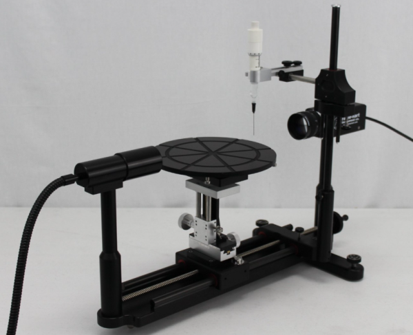
Product of the Month: ramé-hart Model 400

The ramé-hart Model 400 Goniometer / Tensiometer with Wafer Support is an essential tool specifically designed for the semiconductor industry. Its unique construction, including a rotating wafer support, makes it an invaluable tool for ensuring the quality and uniformity of surface preparations, coatings, and primers throughout the entire fabrication process. Key features that make it so compelling are its high-precision contact angle measurement capability, which is critical for assessing wettability, along with its comprehensive DROPimage Pro software that includes a suite of surface energy tools. These features allow semiconductor fabricators to precisely characterize wafer surfaces and identify potential issues like contamination, which is crucial for maximizing yield and device reliability.

Contact us today if you'd like a quotation for our Model 400 or any other model. We look forward to hearing from you.

 
Errata
It appears that there was an error that was introduced to our liquids.txt file in our DROPimage Advanced Software. The error relates the density of glycerol. If you are running DROPimage Advanced and would like to check to see if this error affects your installation, follow these steps:

1. In DROPimage Advanced, click on Edit > Edit Phase Data.
2. Change the Phase File to "Liquids".
3. Scroll down to "Glycerol". If the value reads 1.26, you're good to go.
4. If a different value is reported, then change it to 1.26, click on Save, and then Click on Close. You are now good to go.

We'd like to thank our customers at Argonne National Lab for finding the error.


Regards,

Carl Clegg
Director of Sales
Phone 973-448-0305
www.ramehart.com
Contact us